This post will introduce how to use it as a GPIO board with a clock divider example.
This work will use the following devices:
- ZCU106 FPGA board
- ALINX FH1010 expansion Ports
- Digilent Analog Discovery 2
The software will be used:
- Vivado 2020.2 and petalinux
- Xilinx system controller

Clock divider design
- Create an AXI-Lite IP and modify the axi interface IO. The AXI Lite IP comes with 4 registers and we will use the register 0 to store the the dividend.
1 | module clk_div_v1 ( |
- Modify the AXI IP
1 | module clk_div_v1_S00_AXI( |
Block Design
Create the block as following:
- Add
Clocking WizardIP and set theclk_out1to10MHz. - Create the user constraint file for the generated clock and I/O:
1 | set_property IOSTANDARD LVCMOS18 [get_ports clk_div] |
In this example, we are using the LA23_P I/O port to output the generated clock to the oscilloscope. LA23_P can be used as a single ended I/O and it’s voltage is set to 1.8V. It’s connected to the PIN8 of J2 in the ALINX expansion board.
The connection between the FPGA I/O pin to the expansion board can be found at UG1244 and FL1010 user manual.
Next synthesis the project in Vivado and generate the firmware in Petalinux.
Setup the Vadj of the FPGA
In ZCU106, the configuration of Vadj affects the output voltage of the I/O ports in the expansion board. However, it’s 0V by default. Therefore, we need to use the System Control application (in the pre-request) to configure the ZCU106 before using the I/O ports. This step needs a Windows PC to run the application. To setup the Vadj just click the button
Configuration the Vadj
Boot and Test the IO
The address the memory-mapped register of the clock divider IP is mapped to the 0xA0000000. After booting the fpga (with firmware), ssh into the FPGA.
1 | $ devmem 0xA0000000 w 1000 # write a word to the memory mapped register |
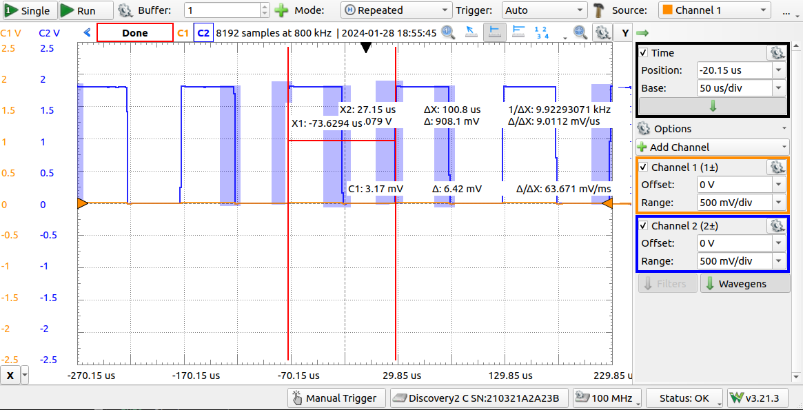
The output looks like this:

